GPD Pocket 3 Cellular Module
TL;DR: I made an LTE/Cellular module for the GPD Pocket 3. If you’re here thinking “where can I buy one?!” feel free to skip all this and just skip to the bottom!
My dad has always been enthusiastic about the Ultra-Mobile PC (UMPC) space, and for almost as long as I can remember, has always been the owner of a UMPC of some form or another.
Lately, that UMPC has been the GPD Pocket 3. The Pocket 3 has an impressive feature set, including an Intel Core i7-1195G7, 16GB of 3733MHz LPDDR4 RAM, and a fast PCIe M.2 SSD.
The G3 Pocket has an expansion port that allows the connection of one of a number of available modules. Currently, all of the modules are manufactured by GPD themselves, and the mechanical/electronic specifications for the expansion modules are not public at time of writing, as far as I am aware.
The current set of available modules comprises:
- USB-A module, which comes with the GPD Pocket 3 as standard
- HDMI/KVM module and a RS-232 9-Way D-Type module (available as a pair for ~£90)
- microSD (aka “TF card”) reader module (scant availability, but still on offer in places for ~£30)
What’s Missing?
Cellular connectivity. In terms of other connectivity, the device ticks almost all the boxes - Wi-Fi 6E & 2.5Gb Ethernet. But when you’re on the road, pulling out a chunky LTE dongle and using up one of your precious two USB A ports really spoils the UMPC vibe.
With this in mind, Dad asked me if there was an option for an internal cellular module.
Can We Make One?
We searched around some more and found that a Chinese user, San, had already had a go at making a module that will fit the Pocket 3’s expansion port. This is a really excellent piece of work, San even made the design files available.
I was tempted to set off manufacturing one based on the design files, but I was a little concerned about the manufacturability, especially around the design involving flat-flex connectors, a discrete antenna, and a few parts that are diffucult to source outside of China.
Having done a fair bit of electronics work involving Cellular modules, I felt confident enough to have a go at designing my own solution.
Design
The architecture of the design is a pretty typical/simplified USB Cellular Module design. A 3A-capable buck converter to convert the 5V USB supply to ~3.8V for the Cellular Module, SIM holder, antenna & matching circuit, plus various bits of support circuitry & protection. The real challenge here ended up being space.
You can view an interactive BOM/layout here.
There’s a lot I can write about designing a piece of electronics like this - more than there’s time to write and read here. I’ve picked a few interesting aspects of the design to write about.
Module Connection
The electrical connectivity for the Pocket 3 modules takes the form of a series of 2.0mm pitch pads on a flex-rigid PCB on the upper side of the module slot. These mate with gold-plated pogo pins on the modules. It was difficult to work out the pinout from San’s designs, so I ended up probing around both the Pocket 3 itself and some of the OEM module. I was eventually able to ascertain which ones I’d need to connect to (USB 5V VBUS, Ground, plus the two differential USB data lines).
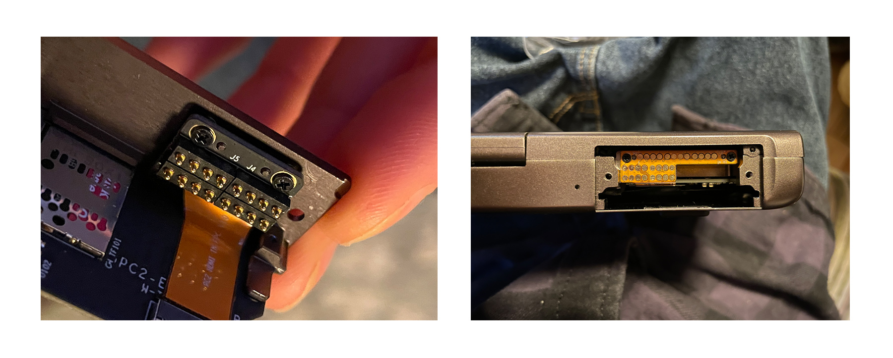
The pogo pins themselves were a nightmare to find. While pins and assemblies are available from the likes of Mill-Max, they are prohibitively expensive, sometimes exceeding £1 per pin. Finding 2.0mm pitch (not the vastly more common 2.54mm/0.1” variety) in exactly the right height with the right mounting type was tricky, but eventually AliExpress delivered the goods.
PCB Assembly
I wanted to produce a connectorless solution to keep the module as low-cost and easy-to-manufacture as possible. In the first revision, the PCB was a two-part snap-off “mousebite” design, which you’ll see in the images of the prototypes I’ve made, but I found that problematic for two reasons. Firstly, the small size meant it was difficult to ensure the design had enough integrity to survive manufacture, but would still break-off without damage. Secondly, it didn’t help the economics of the design at all anyway. JLCPCB were annoyingly smart enough to identify it as two separate boards and rejected my original order; insisting I pay a further fee to cover the second design. Hmph.
After copious amounts of measurement, 3D printed experiments and fiddly adjustments, I had a design I was happy with. The four solderable interlocking tabs of the front-board that mate with the main board carry the USB, Power, Ground, LED & power button signals while also providing rigidity to the design. A single M2 countersink bolt and nut, along with locating tabs fastens the PCBA to the 3D-printed front panel.
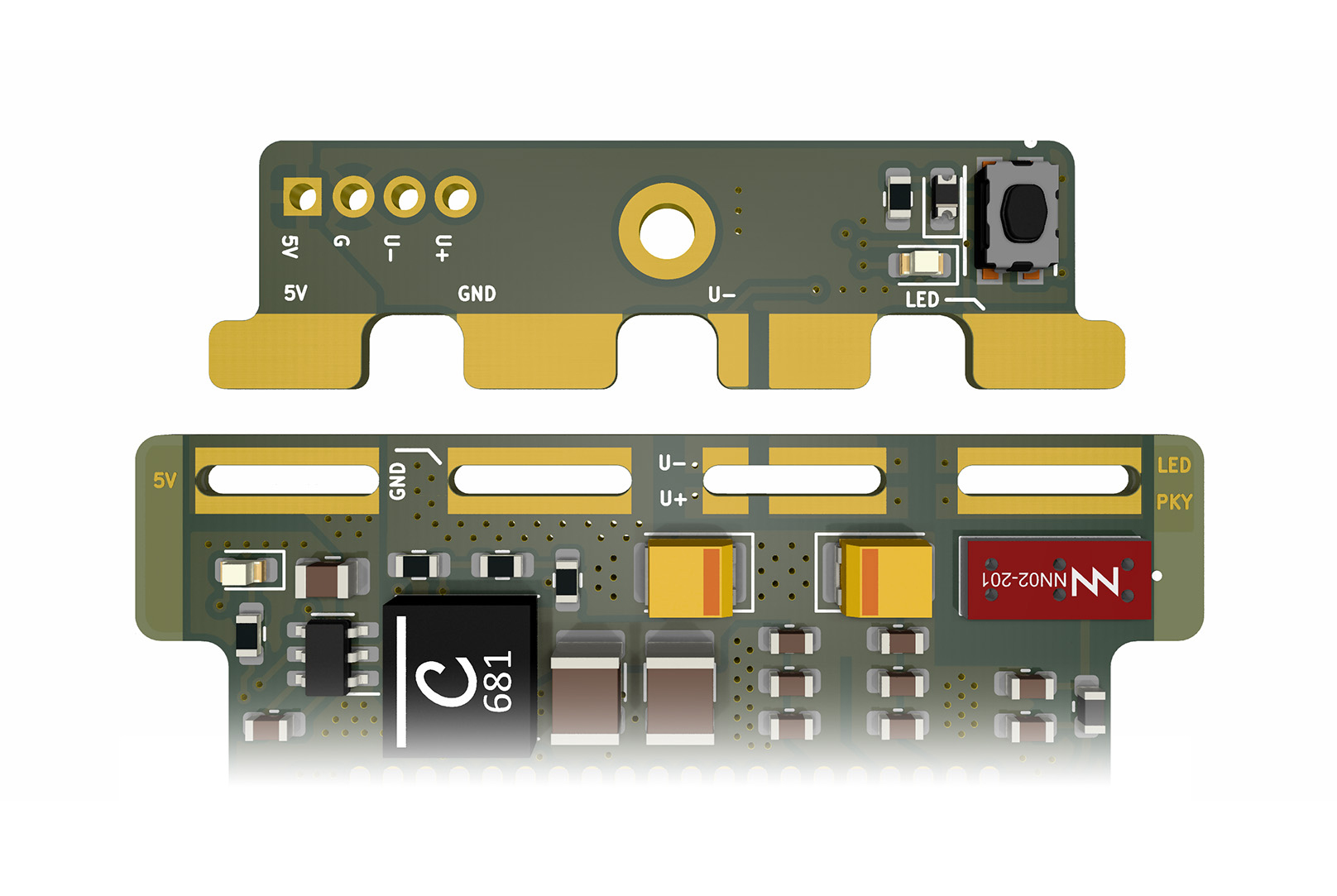
The vertical position and perpendicularity of the front-panel board relative to the main board is important for the alignment of the pogo pins, so I made a small 3D-printed jig to hold them in the correct position during assembly.
Cellular Module Selection
This is one of the most space-constrained cellular designs I’ve ever worked on. I wanted to use at least an LTE Category 4 module for this application since the faster data rates (150Mbps DL, 50Mbps UL) are preferable; but these are larger than their low data rate Category 1 & Category M1 counterparts.
The Quectel EC25 series of modules measures 29mm by 32mm, which is just small enough to fit inside the Pocket 3’s module slot. Quectel also make a lower-cost data-only variant (EC200T) in the same form-factor & pinout. The EC25 also has the benefit of having castellated contacts on the edges rather than being a fiddly BGA backage. There is a large array of ground connections on the bottom of the module, but I used a variation on a trick I learned from mikeselectricstuff to allow those to be soldered from underneath later - add lots of separate pads on the back of the board with many vias through to the pad on the top.
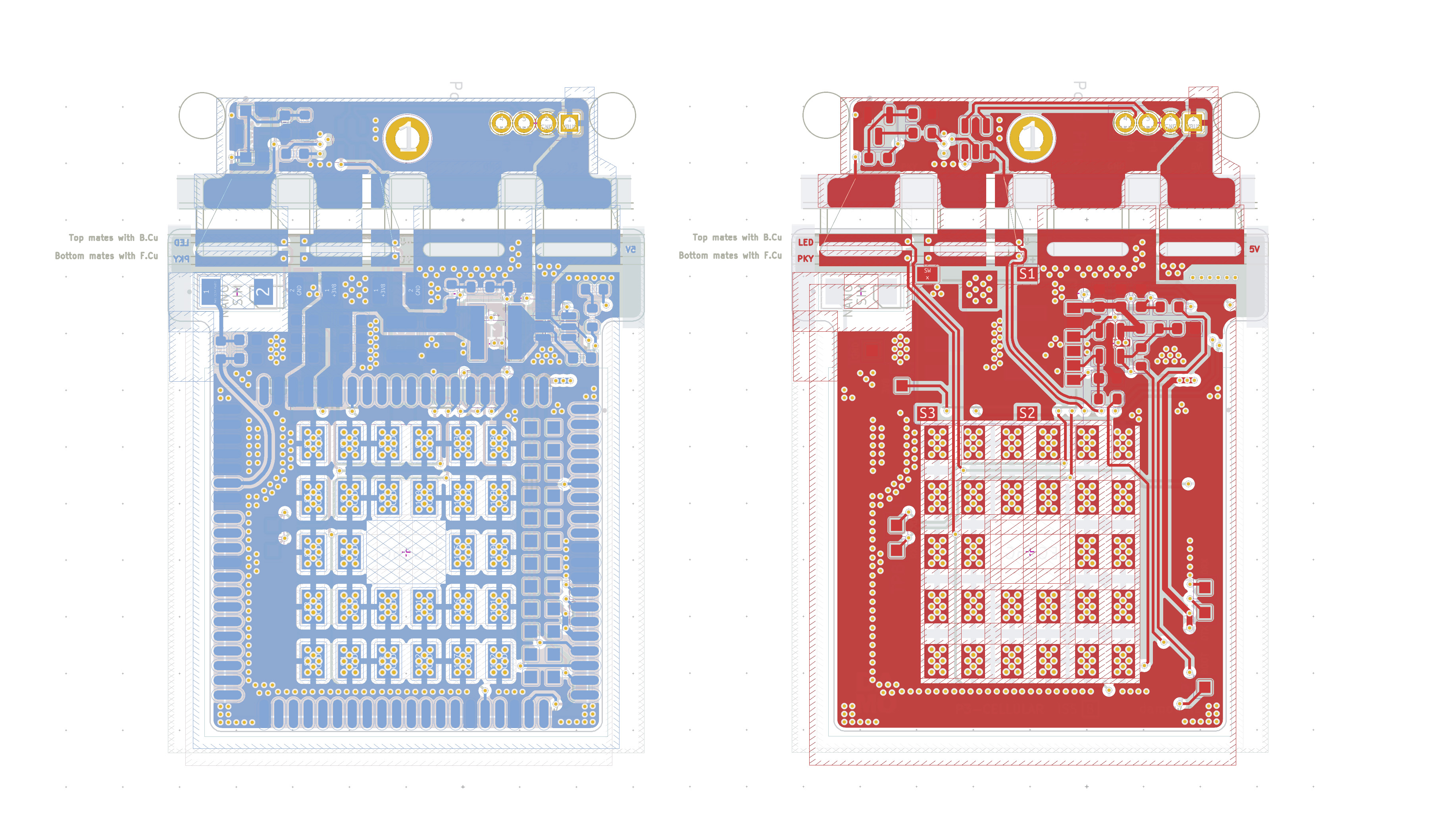
The left image shows the “top” copper layer, on which the EC25 module is mounted. This layer provides the ground connection. The spokes connecting each pad to the copper fill reduce the thermal mass of the connections and make them easier to solder. The right image shows the “bottom” copper layer, which just allows thermal access to the ground pads. This can be done with hot air, or directly with a large-tip iron after the castellated pads are soldered.
The height of the components on the main board had to be carefully controlled to avoid them interfering with the module slot. I saved some more vertical space by opting to fabricate the board using 1.0mm PCB material rather than the standard 1.6mm.
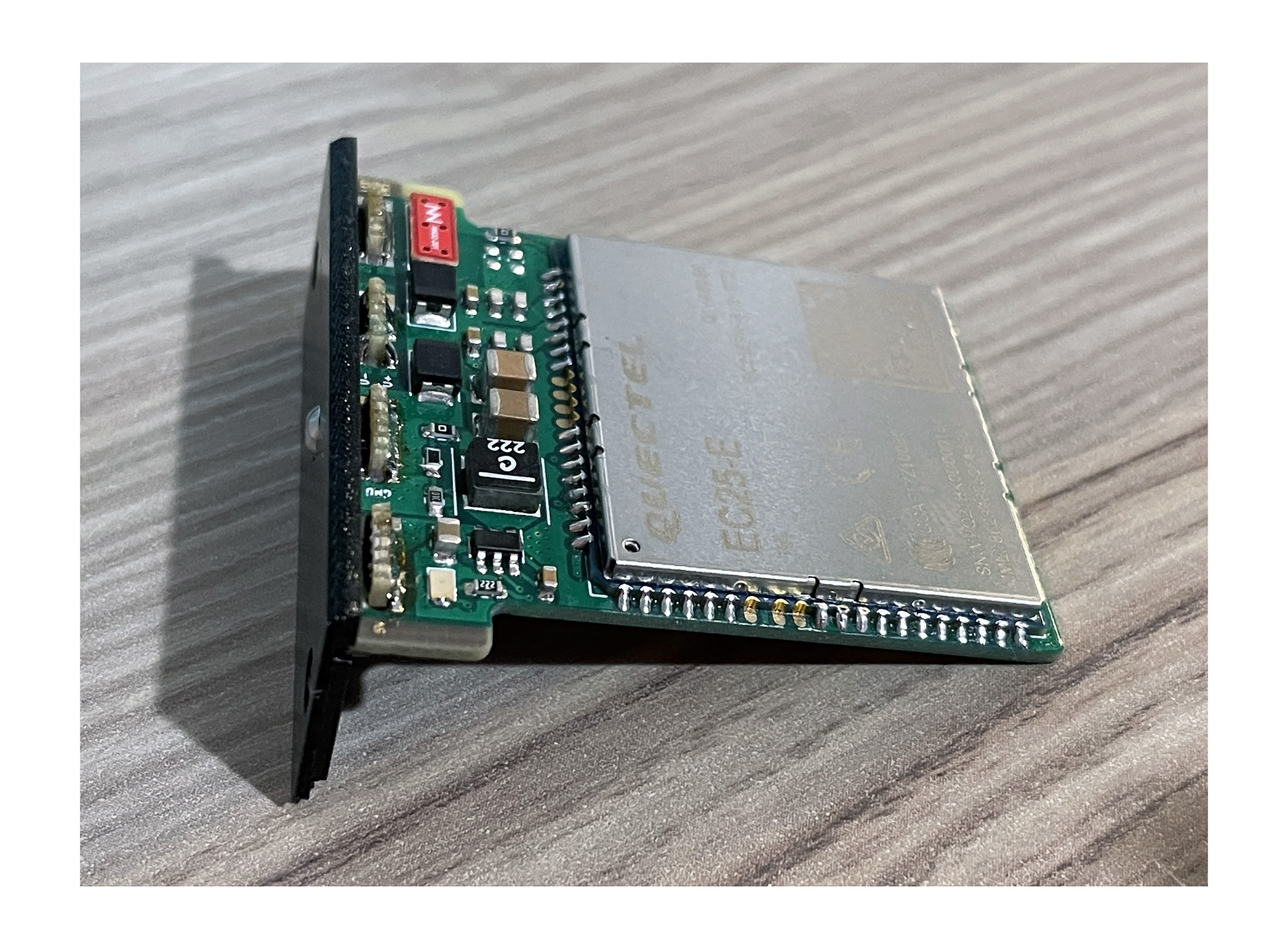
The constrained size of the design necessetated some creative layout, at which I’m sure any serious RF engineers reading will be raising their eyebrows, but it works. I am also sure the tiny surface-mount antenna is sub-optimal compaired to an off-board discrete antenna too, but I feel there’s less to go wrong post-manufacturing with this approach. At some point I’ll need to look into tuning the antenna circuit properly but performance of the initial samples seems adequate.
Design Files
As always, I’ve made the design files available on GitHub. I’m always keen to hear feedback for all of my designs so please do comment below or via GitHub Issues!
So… Can I Buy One?
Maybe! If you’re interested in obtaining a module, feel free to drop me an email and I will do my best to provide. Please do understand however that this is a prototype design being produced in very small volumes, by hand! If there’s sufficient demand, I might be able to arrange a production run with larger volumes.